Understanding PCB Potting Services: Enhancing Performance and Longevity
Understanding PCB Potting Services: Enhancing Performance and Longevity
The protection and longevity of printed circuit boards (PCBs) are paramount in electronics. As technology evolves, the demand for robust and reliable solutions to safeguard PCBs from environmental stresses has increased. This is where PCB potting services come into play. Potting is a method that involves encasing electronic components in a solid or gelatinous compound to protect them from moisture, dust, chemicals, and mechanical shock. This article will delve into the significance of PCB potting services, their benefits, and the various techniques involved.
What is PCB Potting?
PCB potting is a process where electronic assemblies are encased in a protective material. This material is often a thermosetting polymer or silicone designed to create a barrier against environmental factors. Potting serves multiple purposes:
- Protection from moisture:Prevents corrosion and short-circuits.
- Thermal management:Aids in dissipating heat generated by electronic components.
- Mechanical support:Enhances durability and resistance to vibrations.
- Chemical resistance:Protects against harmful substances and solvents.
The Importance of PCB Potting Services
Investing in PCB potting services is crucial for several reasons:
Enhanced Reliability
- Increased Lifespan:Potting significantly extends the life of PCBs by protecting them from environmental hazards.
- Consistent Performance:Encapsulation helps maintain optimal performance even in harsh conditions.
Environmental Protection
- Moisture Barrier:Keeps out humidity and water, which is crucial for outdoor and industrial applications.
- Dust and Contaminants:Protects against particles that could lead to circuit failures.
Improved Thermal Management
- Heat Dissipation:Potting compounds can conduct heat away from critical components, reducing the risk of overheating.
- Thermal Stability:Maintains performance across varying temperatures.
Shock and Vibration Resistance
- Mechanical Support:Potting materials absorb shocks and vibrations, protecting sensitive components.
- Reduced Damage:Minimizes the risk of physical damage during handling and transportation.
Types of Potting Materials
Different types of materials can be used for potting, each with unique properties suited for specific applications:
Epoxy Resins
- Durability:High strength and chemical resistance.
- Curing Process:Can be thermally or chemically cured.
Polyurethane
- Flexibility:Offers better flexibility compared to epoxies.
- Impact Resistance:Good at absorbing shocks and vibrations.
Silicone
- Temperature Tolerance:Excellent for applications with extreme temperatures.
- Electrical Insulation:Provides superior dielectric properties.
Hybrid Materials
- Combines Properties:Mixtures of different materials to achieve desired performance characteristics.
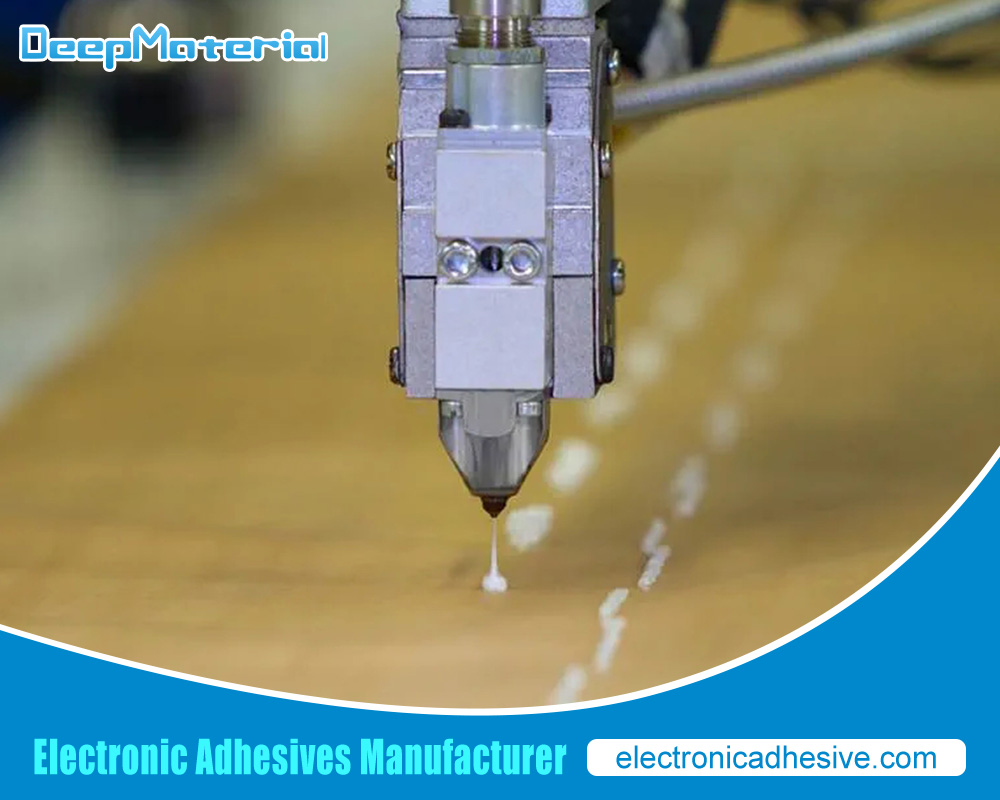
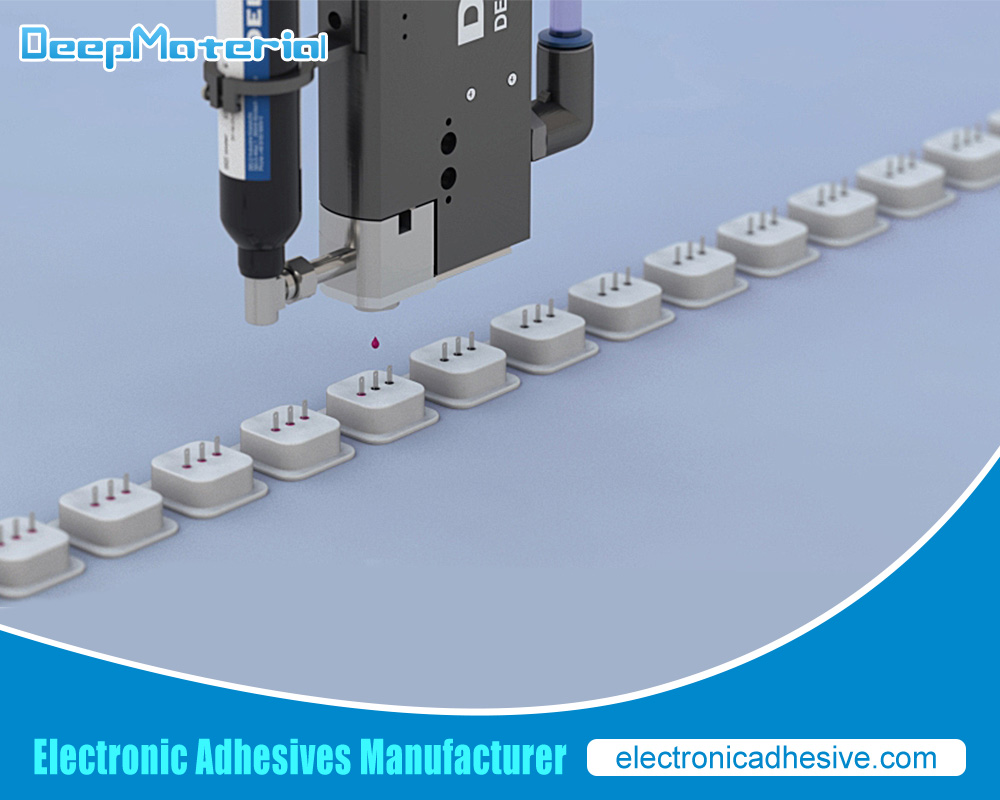
The PCB Potting Process
Understanding the potting process can help businesses choose the right service provider. Here are the typical steps involved:
Preparation
- Cleaning:Ensuring that the PCB is free of contaminants.
- Drying:Eliminating any moisture that could interfere with the potting material.
Selection of Potting Compound
- Choosing the Right Material:Based on the application’s environmental and mechanical requirements.
Application
- Mixing:Preparing the potting compound according to specifications.
- Pouring or Dispensing:Applying the material to ensure complete component coverage.
Curing
- Setting Time:Curing the potting material may involve heat or ambient conditions.
Quality Control
- Testing:Conducting electrical tests to ensure performance.
- Inspection:Checking for any voids or imperfections in the potting.
Benefits of Professional PCB Potting Services
Utilizing professional PCB potting services offers several advantages:
Expertise and Experience
- Skilled Technicians:Trained personnel ensure proper application and curing.
- Best Practices:Knowledge of industry standards and techniques.
Customized Solutions
- Tailored Potting:Services can be adapted to meet specific client needs.
- Material Selection:Professionals can recommend the best materials for the application.
Cost-Effectiveness
- Reduced Failures:Protecting PCBs leads to fewer replacements and repairs.
- Long-Term Investment:Enhances the overall value of electronic products.
Scalability
- Volume Production:Capable of handling small to large production runs efficiently.
- Quick Turnaround:Timely services to meet market demands.
Industries That Benefit from PCB Potting Services
Many sectors leverage PCB potting services to enhance their products. Here are some notable industries:
Automotive
- Electronic Control Units (ECUs):Protects sensitive components from vibrations and harsh environments.
- Sensors:Ensures reliable performance in various weather conditions.
Aerospace
- Critical Systems:Safeguards avionics and other essential electronic systems.
- Reliability Requirements:High standards for safety and performance.
Medical Devices
- Patient Safety:Protects electronic components in devices that interact with patients.
- Sterilization Compatibility:Ensures that potting materials can withstand sterilization processes.
Consumer Electronics
- Durability in Use:Enhances the longevity of products exposed to everyday wear and tear.
- Water Resistance:Essential for devices used in humid or wet environments.
Common Applications of PCB Potting
PCB potting finds applications across a range of products and systems:
Power Supplies
- Voltage Regulation Circuits:Protects against environmental factors and enhances thermal management.
Communication Devices
- Signal Integrity:Maintains performance under varying conditions.
Industrial Equipment
- Control Systems:Provides reliability and robustness in harsh industrial settings.
Home Appliances
- Electronics in Appliances:Protects PCB components from moisture and heat.
Challenges in PCB Potting Services
While PCB potting offers numerous benefits, some challenges need to be addressed:
Material Selection
- Compatibility:Ensuring the potting material does not negatively affect the PCB or components.
- Performance Trade-offs:Balancing flexibility, strength, and thermal conductivity.
Application Techniques
- Uniform Coverage:Consistent potting can be challenging, especially in complex assemblies.
- Curing Time:Managing the curing process to avoid production delays.
Environmental Considerations
- Disposal of Materials:Ensuring that used materials are disposed of or recycled appropriately.
- Sustainability Practices:Using eco-friendly potting materials whenever possible.
Future Trends in PCB Potting Services
The PCB potting industry is continually evolving. Here are some trends to watch for:
Advanced Materials
- Nano-coatings:Development of new materials that provide enhanced protection and functionality.
- Biodegradable Options:Increasing demand for eco-friendly potting materials.
Automation and Technology
- Robotic Applications:Streamlining the potting process for improved efficiency.
- Smart Manufacturing:Integration of IoT for real-time monitoring and quality control.
Customization and Flexibility
- Bespoke Solutions:The trend towards tailor-made potting services to meet specific customer needs.
- Rapid Prototyping:Faster turnaround times for product development cycles.
Conclusion
In summary, PCB potting services enhance electronic components’ reliability, performance, and longevity. As industries continue to evolve, the need for adequate protection against environmental hazards becomes increasingly essential. By understanding the benefits, processes, and future trends associated with PCB potting, businesses can make informed decisions that enhance their products’ performance and reliability. Investing in professional potting services ensures PCBs’ integrity and represents a strategic advantage in the competitive landscape of electronics manufacturing.
For more about understanding PCB potting services: enhancing performance and longevity, you can pay a visit to DeepMaterial at https://www.electronicadhesive.com/ for more info.