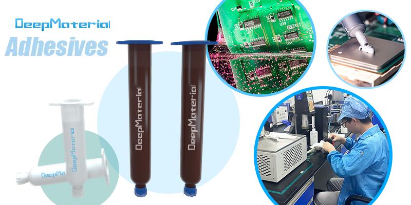
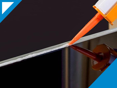
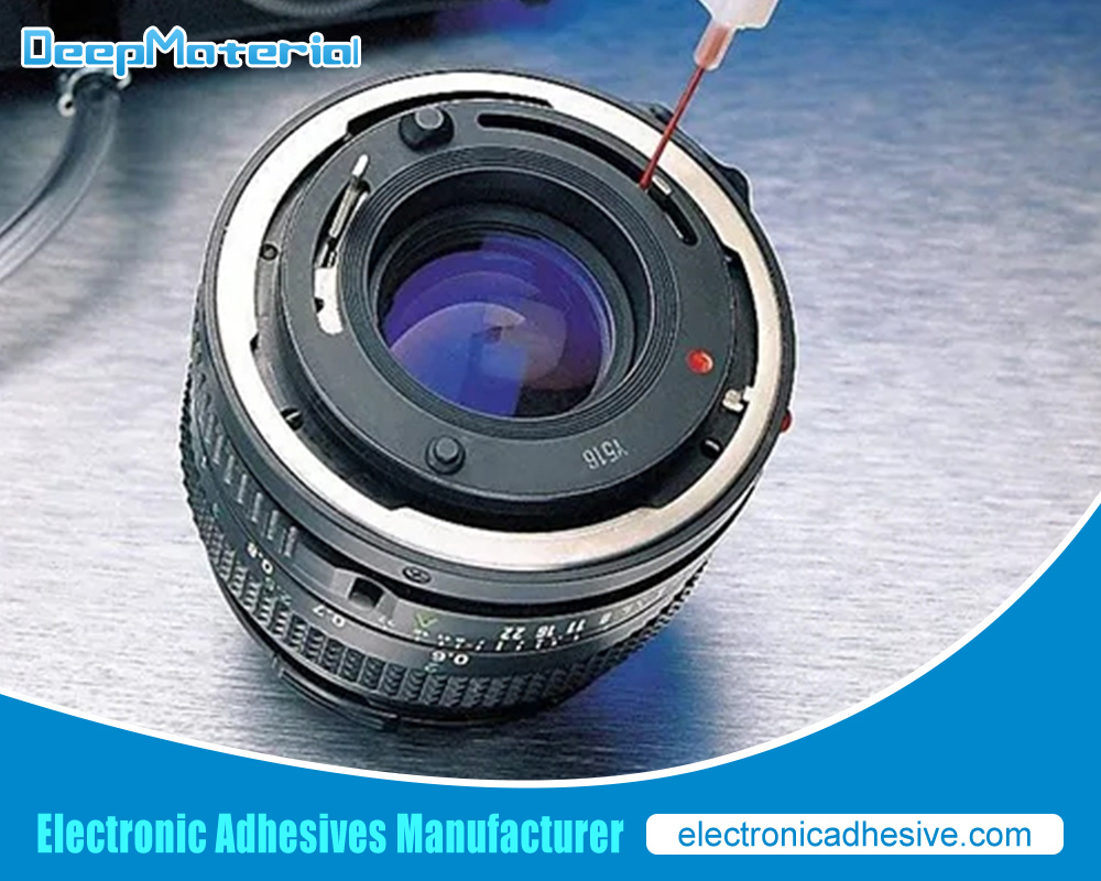
Underfill Epoxy
Underfill epoxy is a type of adhesive used to enhance electronic components’ reliability, particularly in semiconductor packaging applications. It fills the gap between the package and the printed circuit board (PCB), providing mechanical support and stress relief to prevent thermal expansion and contraction damage. Underfill epoxy also improves the electrical performance of the package by reducing the parasitic inductance and capacitance. In this article, we explore the various applications of underfill epoxy, the different types available, and their benefits.
The Importance of Underfill Epoxy in Semiconductor Packaging
Underfill epoxy is crucial in semiconductor packaging, providing mechanical reinforcement and protection to delicate microelectronic components. It is a specialized adhesive material used to fill the gap between the semiconductor chip and the package substrate, enhancing the reliability and performance of electronic devices. Here, we will explore the importance of underfilled epoxy in semiconductor packaging.
One of the primary functions of underfilled epoxy is to improve the mechanical strength and reliability of the package. During operation, semiconductor chips are subjected to various mechanical stresses, such as thermal expansion and contraction, vibration, and mechanical shock. These stresses can lead to the formation of solder joint cracks, which can cause electrical failures and decrease the overall lifespan of the device. Underfill epoxy acts as a stress-reducing agent by distributing the mechanical stress evenly across the chip, substrate, and solder joints. It effectively minimizes the formation of cracks and prevents the propagation of existing cracks, ensuring the long-term reliability of the package.
Another critical aspect of underfill epoxy is its ability to enhance the thermal performance of semiconductor devices. Heat dissipation becomes a significant concern as electronic devices shrink in size and increase power density, and excessive heat can degrade the performance and reliability of the semiconductor chip. Underfill epoxy has excellent thermal conductivity properties, allowing it to efficiently transfer heat from the chip and distribute it throughout the package. This helps maintain optimal operating temperatures and prevents hotspots, thereby improving the overall thermal management of the device.
Underfill epoxy also protects against moisture and contaminants. Moisture ingress can lead to corrosion, electrical leakage, and the growth of conductive materials, resulting in device malfunctions. Underfill epoxy acts as a barrier, sealing vulnerable areas and preventing moisture from entering the package. It also offers protection against dust, dirt, and other contaminants that can adversely affect the electrical performance of the semiconductor chip. By safeguarding the chip and its interconnections, underfill epoxy ensures the long-term reliability and functionality of the device.
Furthermore, underfilled epoxy enables miniaturization in semiconductor packaging. With the constant demand for smaller and more compact devices, underfilled epoxy allows using flip-chip and chip-scale packaging techniques. These techniques involve directly mounting the chip onto the package substrate, eliminating the need for wire bonding and reducing the package size. Underfill epoxy provides structural support and maintains the integrity of the chip-substrate interface, enabling the successful implementation of these advanced packaging technologies.
How Underfill Epoxy Addresses the Challenges
Semiconductor packaging plays a crucial role in electronic device performance, reliability, and longevity. It involves encapsulating integrated circuits (ICs) in protective casings, providing electrical connections, and dissipating heat generated during operation. However, semiconductor packaging faces several challenges, including thermal stress and warpage, which can significantly impact the functionality and reliability of the packaged devices.
One of the primary challenges is thermal stress. Integrated circuits generate heat during operation, and inadequate dissipation can increase temperatures within the package. This temperature variation results in thermal stress as different materials within the package expand and contract at different rates. The non-uniform expansion and contraction can cause mechanical strain, leading to solder joint failures, delamination, and cracks. Thermal stress can compromise the electrical and mechanical integrity of the package, ultimately affecting the performance and reliability of the device.
Warpage is another critical challenge in semiconductor packaging. Warpage refers to the bending or deformation of the package substrate or the entire package. It can occur during the packaging process or due to thermal stress. Warpage is primarily caused by the mismatch in the coefficient of thermal expansion (CTE) between different materials in the package. For example, the CTE of the silicon die, substrate, and mold compound may differ significantly. When subjected to temperature changes, these materials expand or contract at different rates, leading to warpage.
Warpage poses several problems for semiconductor packages:
- It can result in stress concentration points, increasing the likelihood of mechanical failures and reducing the reliability of the box.
- Warpage can lead to difficulties in the assembly process, as it affects the alignment of the package with other components, such as the printed circuit board (PCB). This misalignment can impair electrical connections and cause performance issues.
- Warpage can impact the overall form factor of the package, making it challenging to integrate the device into small form factor applications or densely populated PCBs.
Various techniques and strategies are employed in semiconductor packaging to address these challenges. These include using advanced materials with matching CTEs to minimize thermal stress and warpage. Thermo-mechanical simulations and modeling are conducted to predict the behavior of the package under different thermal conditions. Design modifications, such as introducing stress relief structures and optimized layouts, are implemented to reduce thermal stress and warpage. Additionally, the development of improved manufacturing processes and equipment helps minimize the occurrence of warpage during assembly.
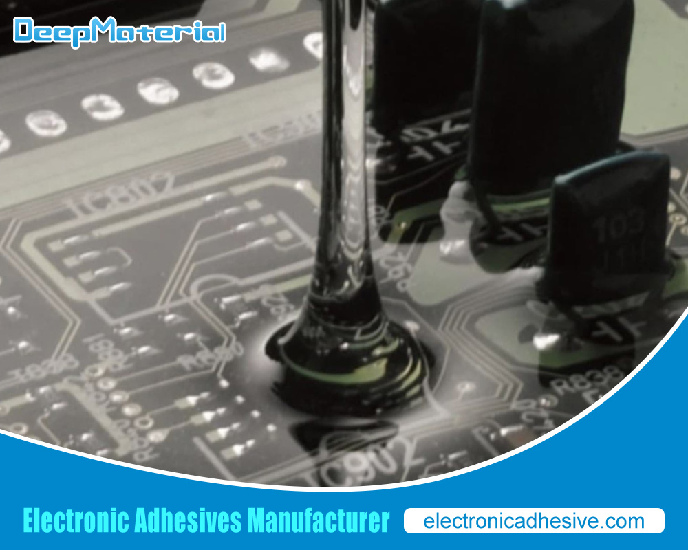
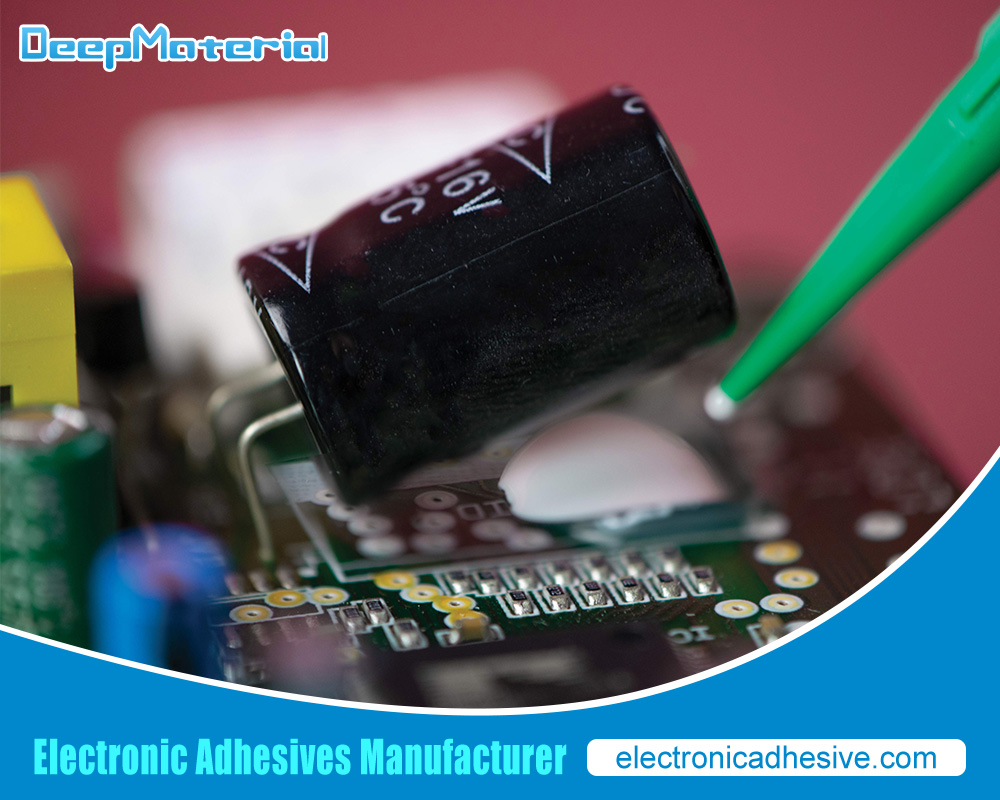
Benefits of Underfill Epoxy
Underfill epoxy is a critical component in semiconductor packaging that offers several benefits. This specialized epoxy material is applied between the semiconductor chip and the package substrate, providing mechanical reinforcement and addressing various challenges. Here are some of the critical benefits of underfilled epoxy:
- Improved Mechanical Reliability: One of the primary benefits of underfill epoxy is its ability to enhance the mechanical reliability of semiconductor packages. Underfill epoxy creates a cohesive bond that improves the overall structural integrity by filling the gaps and voids between the chip and substrate. This helps to prevent package warpage, reduces the risk of mechanical failures, and enhances the resistance to external stresses such as vibrations, shocks, and thermal cycling. The improved mechanical reliability leads to increased product durability and a longer lifespan for the device.
- Thermal Stress Dissipation: Underfill epoxy helps dissipate thermal stress within the package. Integrated circuits generate heat during operation, and inadequate dissipation can result in temperature variations within the container. The underfill epoxy material, with its lower coefficient of thermal expansion (CTE) compared to the chip and substrate materials, acts as a buffer layer. It absorbs the mechanical strain caused by thermal stress, reducing the risk of solder joint failures, delamination, and cracks. By dissipating thermal stress, underfilled epoxy helps maintain the package’s electrical and mechanical integrity.
- Enhanced Electrical Performance: Underfill epoxy positively impacts the electrical performance of semiconductor devices. The epoxy material fills the gaps between the chip and substrate, reducing parasitic capacitance and inductance. This results in improved signal integrity, reduced signal losses, and enhanced electrical connectivity between the chip and the rest of the package. The reduced parasitic effects contribute to better electrical performance, higher data transfer rates, and increased device reliability. Additionally, underfilled epoxy provides insulation and protection against moisture, contaminants, and other environmental factors that can degrade electrical performance.
- Stress Relief and Improved Assembly: Underfill epoxy acts as a stress relief mechanism during assembly. The epoxy material compensates for the CTE mismatch between the chip and substrate, reducing the mechanical stress during temperature changes. This makes the assembly process more reliable and efficient, minimizing the risk of package damage or misalignment. The controlled stress distribution provided by underfill epoxy also helps ensure proper alignment with other components on the printed circuit board (PCB) and improves the overall assembly yield.
- Miniaturization and Form Factor Optimization: Underfill epoxy enables the miniaturization of semiconductor packages and optimization of the form factor. By providing structural reinforcement and stress relief, underfill epoxy allows for designing and manufacturing smaller, thinner, and more compact packages. This is particularly important for applications such as mobile devices and wearable electronics, where space is at a premium. The ability to optimize form factors and achieve higher component densities contributes to more advanced and innovative electronic devices.
Types of Underfill Epoxy
Several types of underfill epoxy formulations are available in semiconductor packaging, each designed to meet specific requirements and address different challenges. Here are some commonly used types of underfill epoxy:
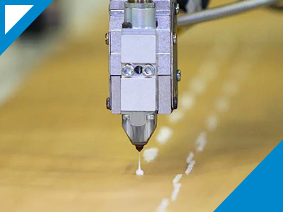
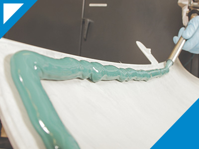
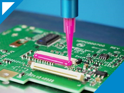
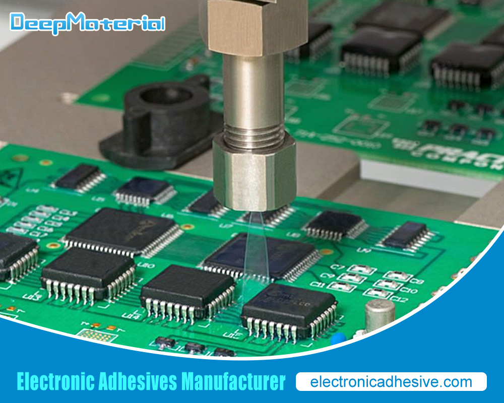
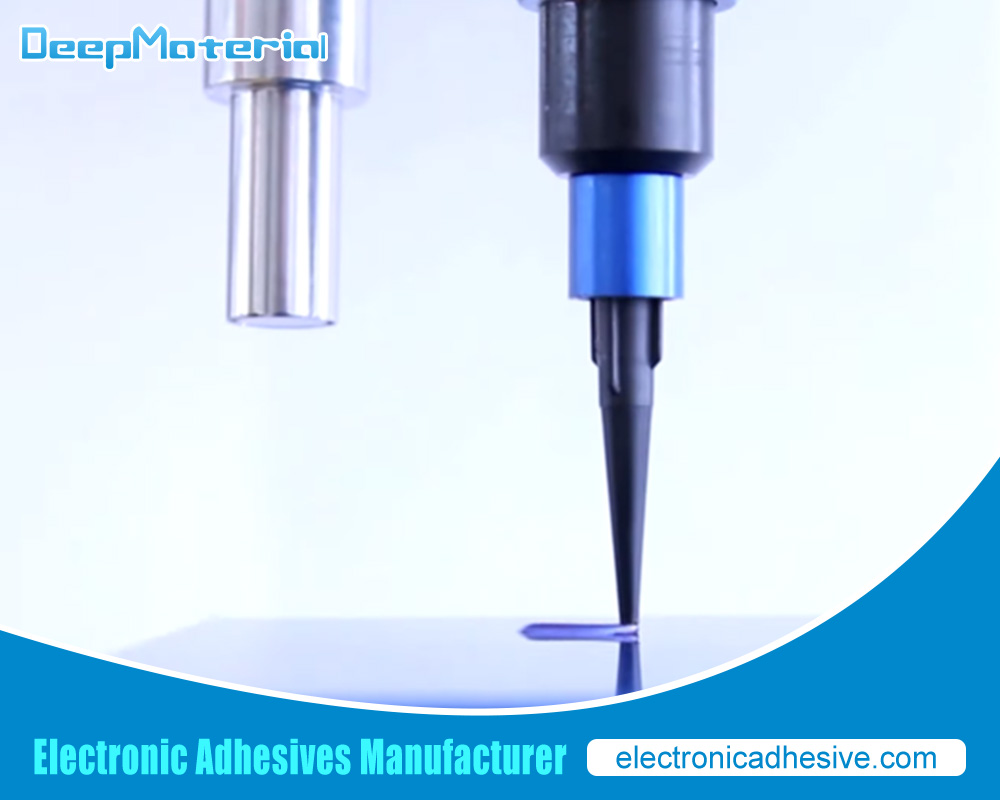
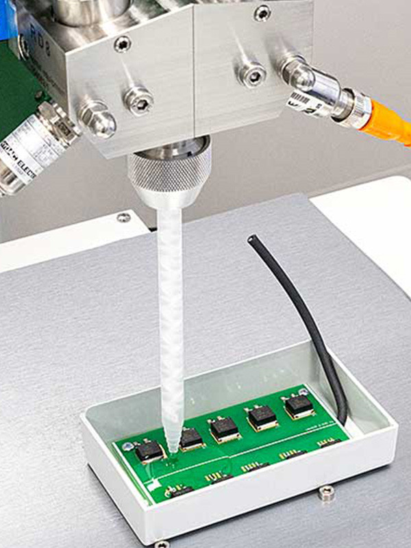
- Capillary Underfill Epoxy: Capillary underfill epoxy is the most traditional and widely used type. A low-viscosity epoxy flows into the gap between the chip and the substrate through capillary action. Capillary underfill is typically dispensed onto the edge of the chip, and as the package is heated, the epoxy flows under the chip, filling the voids. This type of underfill is suitable for packages with small gaps and provides good mechanical reinforcement.
- No-Flow Underfill Epoxy: No-flow underfill epoxy is a high-viscosity formulation that does not flow during curing. It is applied as a pre-applied epoxy or as a film between the chip and the substrate. No-flow underfill epoxy is particularly useful for flip-chip packages, where the solder bumps directly interact with the substrate. It eliminates the need for capillary flow and reduces the risk of solder joint damage during assembly.
- Wafer-Level Underfill (WLU): Wafer-level underfill is an underfill epoxy applied at the wafer level before the individual chips are singulated. It involves dispensing the underfill material over the entire wafer surface and curing it. Wafer-level underfill offers several advantages, including uniform underfill coverage, reduced assembly time, and improved process control. It is commonly used for high-volume manufacturing of small-sized devices.
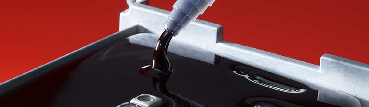
- Molded Underfill (MUF): Molded underfill is an underfill epoxy applied during encapsulation molding. The underfill material is dispensed onto the substrate, and then the chip and substrate are encapsulated in a mold compound. During molding, the epoxy flows and fills the gap between the chip and substrate, providing underfill and encapsulation in a single step. Molded underfill offers excellent mechanical reinforcement and simplifies the assembly process.
- Non-Conductive Underfill (NCF): Non-conductive underfill epoxy is specifically formulated to provide electrical isolation between the solder joints on the chip and the substrate. It contains insulating fillers or additives that prevent electrical conductivity. NCF is used in applications where electrical shorting between adjacent solder joints is a concern. It offers both mechanical reinforcement and electrical isolation.
- Thermally Conductive Underfill (TCU): Thermally conductive underfill epoxy is designed to enhance the heat dissipation capabilities of the package. It contains thermally conductive fillers, such as ceramic or metal particles, that improve the thermal conductivity of the underfill material. TCU is used in applications where efficient heat transfer is crucial, such as high-power devices or those operating in demanding thermal environments.
These are just a few examples of the different types of underfill epoxy used in semiconductor packaging. The selection of the appropriate underfill epoxy depends on factors such as the package design, assembly process, thermal requirements, and electrical considerations. Each underfill epoxy offers specific advantages and is tailored to meet the unique needs of various applications.
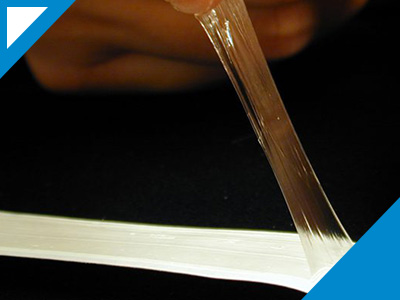
Capillary Underfill: Low Viscosity and High Reliability
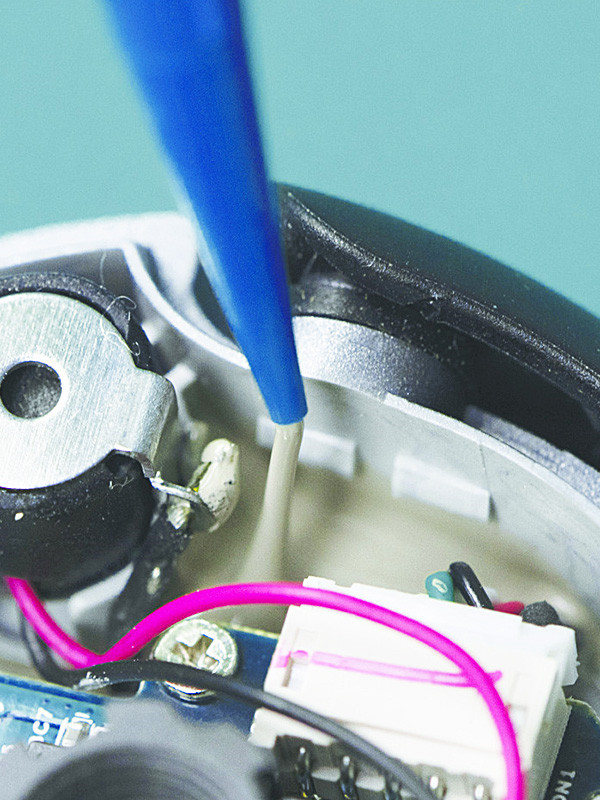
Capillary underfill refers to a process used in the semiconductor packaging industry to enhance the reliability of electronic devices. It involves filling the gaps between a microelectronic chip and its surrounding package with a low-viscosity liquid material, typically an epoxy-based resin. This underfill material provides structural support, improves thermal dissipation, and protects the chip from mechanical stress, moisture, and other environmental factors.
One of the critical characteristics of capillary underfill is its low viscosity. The underfill material is formulated to have a relatively low density, allowing it to flow easily into the narrow gaps between the chip and the package during the underfilling process. This ensures that the underfill material can effectively penetrate and fill all the voids and air gaps, minimizing the risk of void formation and improving the overall integrity of the chip-package interface.
Low-viscosity capillary underfill materials also offer several other advantages. Firstly, they facilitate the efficient flow of the material under the chip, which leads to reduced process time and increased production throughput. This is particularly important in high-volume manufacturing environments where time and cost efficiency are critical.
Secondly, the low viscosity enables better wetting and adhesion properties of the underfill material. It allows the material to spread evenly and form strong bonds with the chip and the package, creating a reliable and robust encapsulation. This ensures the chip is securely protected from mechanical stresses such as thermal cycling, shocks, and vibrations.
Another crucial aspect of capillary underfills is their high reliability. The low-viscosity underfill materials are specifically engineered to exhibit excellent thermal stability, electrical insulation properties, and resistance to moisture and chemicals. These characteristics are essential for ensuring packaged electronic devices’ long-term performance and reliability, particularly in demanding applications such as automotive, aerospace, and telecommunications.
Moreover, capillary underfill materials are designed to have high mechanical strength and excellent adhesion to various substrate materials, including metals, ceramics, and organic materials commonly used in semiconductor packaging. This enables the underfill material to act as a stress buffer, effectively absorbing and dissipating mechanical stresses generated during operation or environmental exposure.
No-Flow Underfill: Self-Dispensing and High Throughput
No-flow underfill a specialized process used in the semiconductor packaging industry to enhance the reliability and efficiency of electronic devices. Unlike capillary underfills, which rely on low-viscosity materials’ flow, no-flow underfills utilize a self-dispensing approach with high-viscosity materials. This method offers several advantages, including self-alignment, high throughput, and improved reliability.
One of the critical features of no-flow underfill is its self-dispensing capability. The underfill material used in this process is formulated with a higher viscosity, which prevents it from flowing freely. Instead, the underfill material is dispensed onto the chip-package interface in a controlled manner. This controlled dispensing enables precise placement of the underfill material, ensuring it is applied only to the desired areas without overflowing or spreading uncontrollably.
The self-dispensing nature of no-flow underfill offers several benefits. Firstly, it allows for self-alignment of the underfill material. As the underfill is dispensed, it naturally self-aligns with the chip and package, filling the gaps and voids uniformly. This eliminates the need for precise positioning and alignment of the chip during the underfilling process, saving time and effort in manufacturing.
Secondly, the self-dispensing feature of no-flow underfills enables high throughput in production. The dispensing process can be automated, allowing for rapid and consistent application of the underfill material across multiple chips simultaneously. This improves the overall production efficiency and reduces manufacturing costs, making it particularly advantageous for high-volume manufacturing environments.
Furthermore, no-flow underfill materials are designed to provide high reliability. The high-viscosity underfill materials offer improved resistance to thermal cycling, mechanical stresses, and environmental factors, ensuring the long-term performance of the packaged electronic devices. The materials exhibit excellent thermal stability, electrical insulation properties, and resistance to moisture and chemicals, contributing to the overall reliability of the devices.
Additionally, the high-viscosity underfill materials used in no-flow underfill have enhanced mechanical strength and adhesion properties. They form strong bonds with the chip and package, effectively absorbing and dissipating mechanical stresses generated during operation or environmental exposure. This helps to protect the chip from potential damage and enhances the device’s resistance to external shocks and vibrations.
Molded Underfill: High Protection and Integration
Molded underfill is an advanced technique used in the semiconductor packaging industry to provide high levels of protection and integration for electronic devices. It involves encapsulating the entire chip and its surrounding package with a mold compound incorporating underfill material. This process offers significant advantages regarding protection, integration, and overall reliability.
One of the critical benefits of molded underfill is its ability to provide comprehensive protection for the chip. The mold compound used in this process acts as a robust barrier, enclosing the entire chip and package in a protective shell. This provides effective shielding against environmental factors such as moisture, dust, and contaminants that could affect the performance and reliability of the device. The encapsulation also helps prevent the chip from mechanical stresses, thermal cycling, and other external forces, ensuring its long-term durability.
Additionally, molded underfill enables high integration levels within the semiconductor package. The underfill material is mixed directly into the mold compound, allowing for seamless integration of the underfill and encapsulation processes. This integration eliminates the need for a separate underfill step, simplifying the manufacturing process and reducing production time and costs. It also ensures consistent and uniform underfill distribution throughout the package, minimizing voids and enhancing the overall structural integrity.
Moreover, molded underfill offers excellent thermal dissipation properties. The mold compound is designed to have high thermal conductivity, allowing it to transfer heat away from the chip efficiently. This is crucial for maintaining the optimal operating temperature of the device and preventing overheating, which can lead to performance degradation and reliability issues. The enhanced thermal dissipation properties of molded underfill contribute to the overall reliability and longevity of the electronic device.
Furthermore, molded underfill enables more miniaturization and form factor optimization. The encapsulation process can be tailored to accommodate various package sizes and shapes, including complex 3D structures. This flexibility allows for integrating multiple chips and other components into a compact, space-efficient package. The ability to achieve higher levels of integration without compromising reliability makes molded underfill particularly valuable in applications where size and weight constraints are critical, such as mobile devices, wearables, and automotive electronics.
Chip Scale Package (CSP) Underfill: Miniaturization and High Density
Chip Scale Package (CSP) underfill is a critical technology enabling miniaturization and high-density electronic device integration. As electronic devices continue to shrink in size while providing increased functionality, CSP underfills a crucial role in ensuring the reliability and performance of these compact devices.
CSP is a packaging technology that allows the semiconductor chip to be directly mounted on the substrate or printed circuit board (PCB) without needing an additional package. This eliminates the need for a traditional plastic or ceramic container, reducing the overall size and weight of the device. CSP underfill a process in which a liquid or encapsulant material is used to fill the gap between the chip and the substrate, providing mechanical support and protecting the chip from environmental factors such as moisture and mechanical stress.
Miniaturization is achieved through CSP underfill by reducing the distance between the chip and the substrate. The underfill material fills the narrow gap between the chip and the substrate, creating a solid bond and improving the mechanical stability of the chip. This allows for smaller and thinner devices, making it possible to pack more functionality into a limited space.
High-density integration is another advantage of CSP underfill. By eliminating the need for a separate package, CSP enables the chip to be mounted closer to other components on the PCB, reducing the length of electrical connections and improving signal integrity. The underfill material also acts as a thermal conductor, efficiently dissipating heat generated by the chip. This thermal management capability allows for higher power densities, enabling the integration of more complex and powerful chips into electronic devices.
CSP underfill materials must possess specific characteristics to meet the demands of miniaturization and high-density integration. They need to have low viscosity to facilitate the filling of narrow gaps, as well as excellent flow properties to ensure uniform coverage and eliminate voids. The materials should also have good adhesion to the chip and the substrate, providing solid mechanical support. Additionally, they must exhibit high thermal conductivity to transfer heat away from the chip efficiently.
Wafer-Level CSP Underfill: Cost-Effective and High Yield
Wafer-level chip scale package (WLCSP) underfill is a cost-effective and high-yield packaging technique that offers several advantages in manufacturing efficiency and overall product quality. WLCSP underfill applies underfill material to multiple chips simultaneously while still in wafer form before they are singulated into individual packages. This approach offers numerous benefits regarding cost reduction, improved process control, and higher production yields.
One of the critical advantages of WLCSP underfill is its cost-effectiveness. Applying the underfill material at the wafer level makes the packaging process more streamlined and efficient. The underfilled material is dispensed onto the wafer using a controlled and automated process, reducing material waste and minimizing labor costs. Additionally, eliminating individual package handling and alignment steps reduces the overall production time and complexity, resulting in significant cost savings compared to traditional packaging methods.
Moreover, WLCSP underfill offers improved process control and higher production yields. Since the underfill material is applied at the wafer level, it enables better control over the dispensing process, ensuring consistent and uniform underfill coverage for each chip on the wafer. This reduces the risk of voids or incomplete underfill, which can lead to reliability issues. The ability to inspect and test the underfill quality at the wafer level also allows for early detection of defects or process variations, enabling timely corrective actions and reducing the likelihood of faulty packages. As a result, WLCSP underfill helps achieve higher production yields and better overall product quality.
The wafer-level approach also enables improved thermal and mechanical performance. The underfill material used in WLCSP is typically a low-viscosity, capillary-flowing material that can efficiently fill the narrow gaps between the chips and the wafer. This provides solid mechanical support to the chips, enhancing their resistance to mechanical stress, vibrations, and temperature cycling. Additionally, the underfill material acts as a thermal conductor, facilitating the dissipation of heat generated by the chips, thus improving thermal management and reducing the risk of overheating.
Flip Chip Underfill: High I/O Density and Performance
Flip chip underfill is a critical technology that enables high input/output (I/O) density and exceptional performance in electronic devices. It plays a crucial role in enhancing the reliability and functionality of flip-chip packaging, which is widely used in advanced semiconductor applications. This article will explore the significance of flip chip underfill and its impact on achieving high I/O density and performance.
Flip chip technology involves the direct electrical connection of an integrated circuit (IC) or a semiconductor die to the substrate, eliminating the need for wire bonding. This results in a more compact and efficient package, as the I/O pads are located on the bottom surface of the die. However, flip-chip packaging presents unique challenges that must be addressed to ensure optimal performance and reliability.
One of the critical challenges in flip chip packaging is preventing mechanical stress and thermal mismatch between the die and the substrate. During the manufacturing process and subsequent operation, the differences in coefficients of thermal expansion (CTE) between the die and substrate can cause significant stress, leading to performance degradation or even failure. Flip chip underfill is a protective material that encapsulates the chip, providing mechanical support and stress relief. It effectively distributes the stresses generated during thermal cycling and prevents them from affecting the delicate interconnects.
High I/O density is critical in modern electronic devices, where smaller form factors and increased functionality are essential. Flip chip underfill enables higher I/O densities by offering superior electrical insulation and thermal management capabilities. The underfill material fills the gap between the die and the substrate, creating a robust interface and reducing the risk of short circuits or electrical leakage. This allows for closer spacing of the I/O pads, resulting in increased I/O density without sacrificing reliability.
Moreover, flip chip underfill contributes to improved electrical performance. It minimizes the electrical parasitics between the die and the substrate, reducing signal delay and enhancing signal integrity. The underfill material also exhibits excellent thermal conductivity properties, efficiently dissipating heat generated by the chip during operation. Effective heat dissipation ensures the temperature remains within acceptable limits, preventing overheating and maintaining optimal performance.
Advancements in flip chip underfill materials have enabled even higher I/O densities and performance levels. Nanocomposite underfills, for instance, leverage nanoscale fillers to enhance thermal conductivity and mechanical strength. This allows for improved heat dissipation and reliability, enabling higher-performance devices.
Ball Grid Array (BGA) Underfill: High Thermal and Mechanical Performance
Ball Grid Array (BGA) underfills a critical technology offering high thermal and mechanical performance in electronic devices. It plays a crucial role in enhancing the reliability and functionality of BGA packages, which are widely used in various applications. In this article, we will explore the significance of BGA underfill and its impact on achieving high thermal and mechanical performance.
BGA technology involves a package design where the integrated circuit (IC) or semiconductor die is mounted on a substrate, and the electrical connections are made through an array of solder balls located on the bottom surface of the package. BGA underfills a material dispensed in the gap between the die and the substrate, encapsulating the solder balls and providing mechanical support and protection to the assembly.
One of the critical challenges in BGA packaging is the management of thermal stresses. During operation, the IC generates heat, and thermal expansion and contraction can cause significant pressure on the solder joints connecting the die and the substrate. BGA underfills a crucial role in mitigating these stresses by forming a solid bond with the die and the substrate. It acts as a stress buffer, absorbing the thermal expansion and contraction and reducing the strain on the solder joints. This helps improve the package’s overall reliability and reduces the risk of solder joint failures.
Another critical aspect of BGA underfill is its ability to enhance the mechanical performance of the package. BGA packages are often subjected to mechanical stresses during handling, assembly, and operation. The underfill material fills the gap between the die and the substrate, providing structural support and reinforcement to the solder joints. This improves the overall mechanical strength of the assembly, making it more resistant to mechanical shocks, vibrations, and other external forces. By effectively distributing the mechanical stresses, BGA underfill helps to prevent package cracking, delamination, or other mechanical failures.
High thermal performance is essential in electronic devices to ensure proper functionality and reliability. BGA underfill materials are designed to have excellent thermal conductivity properties. This allows them to efficiently transfer heat away from the die and distribute it across the substrate, enhancing the overall thermal management of the package. Effective heat dissipation helps to maintain lower operating temperatures, preventing thermal hotspots and potential performance degradation. It also contributes to the box’s longevity by reducing the components’ thermal stress.
Advancements in BGA underfill materials have led to even higher thermal and mechanical performance. Improved formulations and filler materials, such as nanocomposites or high thermal conductivity fillers, have enabled better heat dissipation and mechanical strength, further enhancing the performance of BGA packages.
Quad Flat Package (QFP) Underfill: Large I/O Count and Robustness
Quad Flat Package (QFP) is an integrated circuit (IC) package widely used in electronics. It features a square or rectangular shape with leads extending from all four sides, providing many input/output (I/O) connections. To enhance the reliability and robustness of QFP packages, underfill materials are commonly employed.
Underfill is a protective material applied between the IC and the substrate to reinforce the mechanical strength of the solder joints and prevent stress-induced failures. It is particularly crucial for QFPs with a large I/O count, as the high number of connections can lead to significant mechanical stresses during thermal cycling and operational conditions.
The underfill material used for QFP packages must possess specific characteristics to ensure robustness. Firstly, it should have excellent adhesion to both the IC and the substrate to create a strong bond and minimize the risk of delamination or detachment. Additionally, it should have a low coefficient of thermal expansion (CTE) to match the CTE of the IC and substrate, reducing stress mismatches that could lead to cracks or fractures.
Furthermore, the underfill material should have good flow properties to ensure uniform coverage and complete filling of the gap between the IC and the substrate. This helps in eliminating voids, which can weaken the solder joints and result in reduced reliability. The material should also have good curing properties, allowing it to form a rigid and durable protective layer after application.
In terms of mechanical robustness, the underfill should possess high shear and peel strength to withstand external forces and prevent package deformation or separation. It should also exhibit good resistance to moisture and other environmental factors to maintain its protective properties over time. This is particularly important in applications where the QFP package may be exposed to harsh conditions or undergo temperature variations.
Various underfill materials are available to achieve these desired characteristics, including epoxy-based formulations. Depending on the application’s specific requirements, these materials can be dispensed using different techniques, such as capillary flow, jetting, or screen printing.
System-in-Package (SiP) Underfill: Integration and Performance
System-in-Package (SiP) is an advanced packaging technology integrating multiple semiconductor chips, passive components, and other elements into a single package. SiP offers numerous advantages, including reduced form factor, improved electrical performance, and enhanced functionality. To ensure the reliability and performance of SiP assemblies, underfill materials are commonly used.
Underfill in SiP applications is crucial in providing mechanical stability and electrical connectivity between the various components within the package. It helps to minimize the risk of stress-induced failures, such as solder joint cracks or fractures, which can occur due to differences in coefficients of thermal expansion (CTE) between the components.
Integrating multiple components in a SiP package leads to complex interconnectivity, with many solder joints and high-density circuitry. Underfill materials help to reinforce these interconnections, enhancing the mechanical strength and reliability of the assembly. They support the solder joints, reducing the risk of fatigue or damage caused by thermal cycling or mechanical stress.
In terms of electrical performance, underfill materials are critical in improving signal integrity and minimizing electrical noise. By filling the gaps between components and reducing the distance between them, underfill helps to reduce parasitic capacitance and inductance, enabling faster and more efficient signal transmission.
Additionally, underfill materials for SiP applications should have excellent thermal conductivity to dissipate heat generated by the integrated components efficiently. Effective heat dissipation is essential to prevent overheating and maintain the overall reliability and performance of the SiP assembly.
Underfill materials in SiP packaging must have specific properties to meet these integration and performance requirements. They should have good flowability to ensure complete coverage and fill gaps between the components. The underfill material should also have a low-viscosity formulation to allow easy dispensing and filling in narrow holes or small spaces.
Furthermore, the underfill material should exhibit strong adhesion to different surfaces, including semiconductor chips, substrates, and passives, to ensure reliable bonding. It should be compatible with various packaging materials, such as organic substrates or ceramics, and exhibit good mechanical properties, including high shear and peel strength.
The underfill material and application method choice depends on the specific SiP design, component requirements, and manufacturing processes. Dispensing techniques such as capillary flow, jetting, or film-assisted methods commonly apply underfill in SiP assemblies.
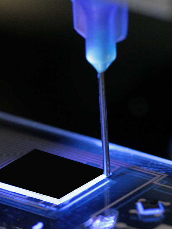
Optoelectronics Underfill: Optical Alignment and Protection
Optoelectronics underfill includes encapsulating and protecting optoelectronic devices while ensuring precise optical alignment. Optoelectronic devices, such as lasers, photodetectors, and optical switches, often require delicate alignment of optical components to achieve optimal performance. At the same time, they need to be protected from environmental factors that could affect their functionality. Optoelectronics underfill addresses both these requirements by providing optical alignment and protection in a single process.
Optical alignment is a critical aspect of optoelectronic device manufacturing. It involves aligning visual elements, such as fibers, waveguides, lenses, or gratings, to ensure efficient light transmission and reception. Precise alignment is necessary to maximize device performance and maintain signal integrity. Traditional alignment techniques include manual alignment using visual inspection or automated alignment using alignment stages. However, these methods can be time-consuming, labor-intensive, and prone to errors.
Optoelectronics underfill an innovative solution by incorporating alignment features directly into the underfill material. Underfill materials are typically liquid or semi-liquid compounds that can flow and fill the gaps between optical components. By adding alignment features, such as microstructures or fiducial marks, within the underfill material, the alignment process can be simplified and automated. These features act as guides during assembly, ensuring precise alignment of the optical components without the need for complex alignment procedures.
In addition to optical alignment, underfill materials protect optoelectronic devices. Optoelectronic components are often exposed to harsh environments, including temperature fluctuations, moisture, and mechanical stress. These external factors can degrade the performance and reliability of the devices over time. Underfill materials act as a protective barrier, encapsulating the optical components and shielding them from environmental contaminants. They also provide mechanical reinforcement, reducing the risk of damage due to shock or vibration.
Underfill materials used in optoelectronics applications are typically designed to have low refractive index and excellent optical transparency. This ensures minimal interference with the optical signals passing through the device. Additionally, they exhibit good adhesion to various substrates and have low thermal expansion coefficients to minimize the device’s stress during thermal cycling.
The underfill process involves dispensing the underfill material onto the device, allowing it to flow and fill the gaps between optical components, and then curing it to form a solid encapsulation. Depending on the specific application, the underfill material can be applied using different techniques, such as capillary flow, jet dispensing, or screen printing. The curing process can be achieved through heat, UV radiation, or both.
Medical Electronics Underfill: Biocompatibility and Reliability
Medical electronics underfill a specialized process that involves encapsulating and protecting electronic components used in medical devices. These devices play a crucial role in various medical applications, such as implantable devices, diagnostic equipment, monitoring systems, and drug delivery systems. Medical electronics underfill focuses on two critical aspects: biocompatibility and reliability.
Biocompatibility is a fundamental requirement for medical devices that come into contact with the human body. The underfill materials used in medical electronics must be biocompatible, meaning they should not cause harmful effects or adverse reactions when in contact with living tissue or bodily fluids. These materials should comply with strict regulations and standards, such as ISO 10993, which specifies biocompatibility testing and evaluation procedures.
Underfill materials for medical electronics are carefully selected or formulated to ensure biocompatibility. They are designed to be non-toxic, non-irritating, and non-allergenic. These materials should not leach any harmful substances or degrade over time, as this could lead to tissue damage or inflammation. Biocompatible underfill materials also have low water absorption to prevent the growth of bacteria or fungi that could cause infections.
Reliability is another critical aspect of medical electronics underfill. Medical devices often face challenging operating conditions, including temperature extremes, moisture, bodily fluids, and mechanical stress. Underfill materials must protect the electronic components, ensuring their long-term reliability and functionality. Reliability is paramount in medical applications where device failure could severely affect patient safety and well-being.
Underfill materials for medical electronics should have high resistance to moisture and chemicals to withstand exposure to bodily fluids or sterilization processes. They should also exhibit good adhesion to various substrates, ensuring secure encapsulation of the electronic components. Mechanical properties, such as low coefficients of thermal expansion and good shock resistance, are crucial to minimizing stress on the details during thermal cycling or automatic loading.
The underfill process for medical electronics involves:
- Dispensing the underfill material onto the electronic components.
- Filling the gaps.
- Curing it to form a protective and mechanically stable encapsulation.
Care must be taken to ensure complete coverage of the features and the absence of voids or air pockets that could compromise the device’s reliability.
Furthermore, additional considerations are taken into account when underfilling medical devices. For example, the underfill material should be compatible with the sterilization methods used for the device. Some materials may be sensitive to specific sterilization techniques, such as steam, ethylene oxide, or radiation, and alternative materials may need to be selected.
Aerospace Electronics Underfill: High Temperature and Vibration Resistance
Aerospace electronics underfill a specialized process to encapsulate and protect electronic components in aerospace applications. Aerospace environments pose unique challenges, including high temperatures, extreme vibrations, and mechanical stresses. Therefore, aerospace electronics underfill focuses on two crucial aspects: high-temperature resistance and vibration resistance.
High-temperature resistance is paramount in aerospace electronics due to the elevated temperatures experienced during operation. The underfill materials used in aerospace applications must withstand these high temperatures without compromising the performance and reliability of the electronic components. They should exhibit minimal thermal expansion and remain stable over a wide temperature range.
Underfill materials for aerospace electronics are selected or formulated for high glass transition temperatures (Tg) and thermal stability. A high Tg ensures that the material retains its mechanical properties at elevated temperatures, preventing deformation or loss of adhesion. These materials can withstand temperature extremes, such as during takeoff, atmospheric reentry, or operating in hot engine compartments.
Additionally, underfill materials for aerospace electronics should have low coefficients of thermal expansion (CTE). The CTE measures how much a material expands or contracts with temperature changes. By having a low CTE, underfill materials can minimize the stress on the electronic components caused by thermal cycling, which can lead to mechanical failures or solder joint fatigue.
Vibration resistance is another critical requirement for aerospace electronics underfill. Aerospace vehicles are subject to various vibrations, including engine, flight-induced vibrations, and mechanical shocks during launch or landing. These vibrations can jeopardize the performance and reliability of electronic components if not adequately protected.
Underfill materials used in aerospace electronics should exhibit excellent vibration-damping properties. They should absorb and dissipate the energy generated by vibrations, reducing the stress and strain on the electronic components. This helps prevent the formation of cracks, fractures, or other mechanical failures due to excessive vibration exposure.
Moreover, underfill materials with high adhesion and cohesive strength are preferred in aerospace applications. These properties ensure the underfill material remains firmly bonded to the electronic components and substrate, even under extreme vibration conditions. Strong adhesion prevents the underfill material from delaminating or separating from the elements, maintaining the integrity of the encapsulation and protecting against moisture or debris ingress.
The underfill process for aerospace electronics typically involves dispensing the underfill material onto the electronic components, allowing it to flow and fill the gaps, and then curing it to form a robust encapsulation. The curing process can be accomplished using thermal or UV curing methods, depending on the application’s specific requirements.
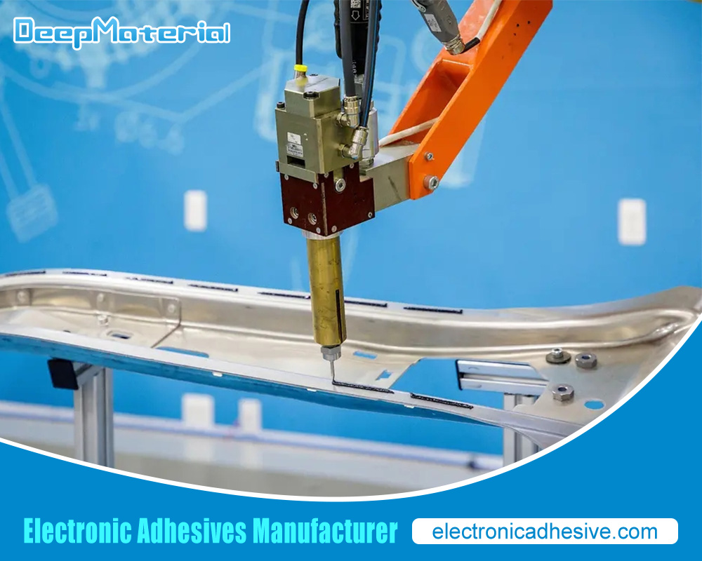
Automotive Electronics Underfill: Durability and Thermal Cycling Resistance
Automotive electronics underfill a critical process that involves encapsulating and protecting electronic components in automotive applications. Automotive environments present unique challenges, including temperature variations, thermal cycling, mechanical stresses, and exposure to moisture and chemicals. Therefore, automotive electronics underfill focuses on two critical aspects: durability and thermal cycling resistance.
Durability is a crucial requirement for automotive electronics underfill. During regular operation, automotive vehicles experience constant vibrations, shocks, and mechanical stresses. The underfill materials used in automotive applications must protect electronic components robustly, ensuring their durability and longevity. They should withstand the harsh conditions and mechanical loads encountered on the road and resist the ingress of moisture, dust, and chemicals.
Underfill materials for automotive electronics are selected or formulated for high mechanical strength and impact resistance. They should exhibit excellent adhesion to the electronic components and substrate, preventing delamination or separation under mechanical stresses. Durable underfill materials help minimize the risk of damage to the electronic components due to vibrations or shocks, ensuring reliable performance over the vehicle’s lifetime.
Thermal cycling resistance is another critical requirement for automotive electronics underfill. Automotive vehicles undergo frequent temperature variations, especially during engine startup and operation, and these temperature cycles can induce thermal stresses on electronic components and the surrounding underfill material. The underfill materials used in automotive applications must have excellent thermal cycling resistance to withstand these temperature fluctuations without compromising their performance.
Underfill materials for automotive electronics should have low thermal expansion (CTE) coefficients to minimize the electronic components’ stress during thermal cycling. A well-matched CTE between the underfill material and the ingredients reduces the risk of solder joint fatigue, cracking, or other mechanical failures caused by thermal stress. Additionally, the underfill materials should exhibit good thermal conductivity to dissipate heat efficiently, preventing localized hotspots that could impact the performance and reliability of the components.
Moreover, automotive electronics underfill materials should resist moisture, chemicals, and fluids. They should have low water absorption to prevent mold growth or corrosion of the electronic components. Chemical resistance ensures that the underfill material remains stable when exposed to automotive fluids, such as oils, fuels, or cleaning agents, avoiding degradation or loss of adhesion.
The underfill process for automotive electronics typically involves dispensing the underfill material onto the electronic components, allowing it to flow and fill the gaps, and then curing it to form a durable encapsulation. The curing process can be accomplished through thermal or UV curing methods, depending on the application’s specific requirements and the underfill material used.
Choosing the Right Underfill Epoxy
Choosing the right underfill epoxy is a crucial decision in the assembly and protection of electronic components. Underfill epoxies provide mechanical reinforcement, thermal management, and protection against environmental factors. Here are some key considerations when selecting the appropriate underfill epoxy:
- Thermal Properties: One of the primary functions of underfill epoxy is dissipating heat generated by electronic components. Therefore, it is essential to consider the epoxy’s thermal conductivity and thermal resistance. High thermal conductivity helps efficient heat transfer, preventing hotspots and maintaining component reliability. The epoxy should also have low thermal resistance to minimize thermal stress on the components during temperature cycling.
- CTE Match: The underfill epoxy’s thermal expansion coefficient (CTE) should be well-matched with the CTE of the electronic components and the substrate to minimize thermal stress and prevent solder joint failures. A closely matched CTE helps to reduce the risk of mechanical failures due to thermal cycling.
- Flow and Gap-Filling Ability: The underfilled epoxy should have good flow characteristics and the ability to fill gaps between components effectively. This ensures complete coverage and minimizes voids or air pockets that could affect the assembly’s mechanical stability and thermal performance. The viscosity of the epoxy should be suitable for the specific application and assembly method, whether it’s capillary flow, jet dispensing, or screen printing.
- Adhesion: Strong adhesion is crucial for underfilling epoxy to ensure reliable bonding between the components and the substrate. It should exhibit good adhesion to various materials, including metals, ceramics, and plastics. The epoxy’s adhesion properties contribute to the assembly’s mechanical integrity and long-term reliability.
- Curing Method: Consider the curing method that best suits your manufacturing process. Underfill epoxies can be cured through heat, UV radiation, or a combination of both. Each curing method has advantages and limitations, and choosing the one that aligns with your production requirements is essential.
- Environmental Resistance: Evaluate the underfill epoxy’s resistance to environmental factors such as moisture, chemicals, and temperature extremes. The epoxy should be able to withstand exposure to water, preventing the growth of mold or corrosion. Chemical resistance ensures stability when in contact with automotive fluids, cleaning agents, or other potentially corrosive substances. Additionally, the epoxy should maintain its mechanical and electrical properties over a wide temperature range.
- Reliability and Longevity: Consider the underfill epoxy’s track record and reliability data. Look for epoxy materials tested and proven to perform well in similar applications or have industry certifications and compliance with relevant standards. Consider factors like aging behavior, long-term reliability, and the epoxy’s ability to maintain its properties over time.
When selecting the right underfill epoxy, it is crucial to consider the specific requirements of your application, including thermal management, mechanical stability, environmental protection, and manufacturing process compatibility. Consulting with epoxy suppliers or seeking expert advice can be beneficial in making an informed decision that meets your application’s needs and ensures optimal performance and reliability.
Future Trends in Underfill Epoxy
Underfill epoxy is continuously evolving, driven by advancements in electronic technologies, emerging applications, and the need for improved performance and reliability. Several future trends can be observed in the development and application of underfill epoxy:
- Miniaturization and Higher Density Packaging: As electronic devices continue to shrink and feature higher component densities, underfill epoxies must adapt accordingly. Future trends will focus on developing underfill materials that penetrate and fill smaller gaps between components, ensuring complete coverage and reliable protection in increasingly miniaturized electronic assemblies.
- High-Frequency Applications: With the growing demand for high-frequency and high-speed electronic devices, underfill epoxy formulations will need to address the specific requirements of these applications. Underfill materials with low dielectric constant and low loss tangents will be essential to minimize signal loss and maintain the integrity of high-frequency signals in advanced communication systems, 5G technology, and other emerging applications.
- Enhanced Thermal Management: Heat dissipation remains a critical concern for electronic devices, especially with the increasing power densities. Future underfill epoxy formulations will focus on improved thermal conductivity to enhance heat transfer and manage thermal issues effectively. Advanced fillers and additives will be incorporated into underfill epoxies to achieve higher thermal conductivity while maintaining other desired properties.
- Flexible and Stretchable Electronics: The rise of flexible and stretchable electronics opens up new possibilities for underfilling epoxy materials. Flexible underfill epoxies must demonstrate excellent adhesion and mechanical properties even under repeated bending or stretching. These materials will enable the encapsulation and protection of electronics in wearable devices, bendable displays, and other applications requiring mechanical flexibility.
- Environmentally Friendly Solutions: Sustainability and environmental considerations will play an increasingly significant role in the development of underfill epoxy materials. There will be a focus on creating epoxy formulations free from hazardous substances and have reduced environmental impact throughout their lifecycle, including manufacturing, usage, and disposal. Bio-based or renewable materials may also gain prominence as sustainable alternatives.
- Improved Manufacturing Processes: Future trends in underfill epoxy will focus on material properties and advancements in manufacturing processes. Techniques such as additive manufacturing, selective dispensing, and advanced curing methods will be explored to optimize the application and performance of underfill epoxy in various electronic assembly processes.
- Integration of Advanced Testing and Characterization Techniques: With the increasing complexity and requirements of electronic devices, there will be a need for advanced testing and characterization methods to ensure the reliability and performance of underfilled epoxy. Techniques such as non-destructive testing, in-situ monitoring, and simulation tools will aid in the development and quality control of underfilled epoxy materials.
Conclusion
Underfill epoxy plays a critical role in enhancing the reliability and performance of electronic components, particularly in semiconductor packaging. The different types of underfill epoxy offer a range of benefits, including high reliability, self-dispensing, high density, and high thermal and mechanical performance. Choosing the right underfill epoxy for the application and package ensures a robust and long-lasting bond. As technology advances and package sizes shrink, we expect even more innovative underfill epoxy solutions offering superior performance, integration, and miniaturization. Underfill epoxy is set to play an increasingly important role in the future of electronics, enabling us to achieve higher levels of reliability and performance in various industries.